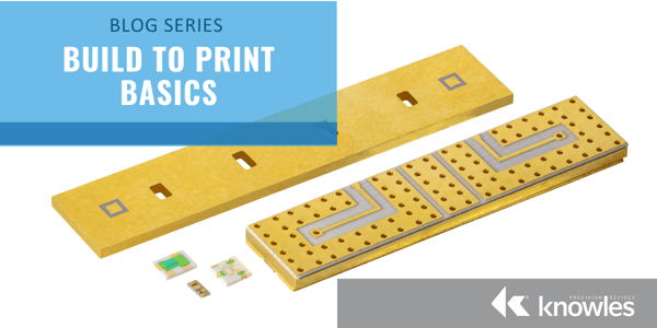
Introduction to Build-to-Print
Learn more about our build-to-print services that facilitate thin-film product design, manufacturing and testing from prototype to high-volume production.
At Knowles Precision Devices, we are not trying to be your typical commodity component manufacturer. We want to do things that are hard and help customers solve their most difficult engineering challenges. This is why we offer build-to-print services to facilitate thin-film product design, manufacturing and testing from prototype to high-volume production.
To provide a better understanding of build-to-print in general and the breadth of our offerings, as well as how our thin-film technology can benefit your applications, we’ve put together a Build-to-Print Basics series.

Table of Contents
Choose a topic of interest ranging from capacitor basics to dielectric types to user guidelines.
Part 1 – An Introduction to Build-to-Print and Thin-Film Technology
Part 1 starts by providing a brief overview of how we approach build-to-print and what thin-film technology actually is.
Part 2 – Build to Print and Custom Thin-Film
In Part 2 of our Build-to-Print Basics Series, we will look at how our custom build-to-print services can provide customers with an even higher level of support and customization for the most complex applications.
Part 3 – Typical Applications for Thin-Film
Part 3 provides an overview of the two broad types of applications where build-to-print designs using thin-film technology offer more reliable options versus off-the-shelf solutions.
Part 4 – The Knowles Precision Devices Build-to-Print Process
Part 4 provides an overview of our process and the topics our applications engineers review with clients to kick-off any build-to-print project.
Part 5 – Substrate Selection
Part 5 provides an overview of the common and custom materials we typically use and information on how we can work together to determine the best substrate option for your application.
Part 6 – Metallization
Part 6 covers the various aspects of metallization that we consider to determine the best fit for our customer’s build-to-print applications.
Part 7 –Laser Techniques
Part 7 covers how we use in-house laser machining, laser trimming, and other laser cutting techniques to build high-precision thin-film components.
Part 8 –Conductors
Part 8 provides basic and multilayer conductor guidelines as well as information on fine line conductor features.
Part 9 –Vias
Part 9 covers the various strategies that can be used for adding vias into circuits.
Part 10 –Resistors
Part 10 covers our key design parameters for resistors as well as our standard layouts.
Part 11 –Supported Bridges and Solder Dams
Part 11 covers how we work with solder, solder masks, and supported bridges in the thin-film components we design and develop.
Part 12 – Custom Microwave Components
Part 12 ties everything we’ve discussed so far together and provides more specifics about how we use the processes and options detailed throughout this series to create the custom microwave components you need.
Part 13 – Bias Networks
Part 13 provides an overview of how we use our build-to-print process and thin-film expertise to develop bias networks that support the functionality of active microwave components while also minimizing the space needed in a circuit for certain components and simplifying circuit assembly.
Part 14 – Testing
Part 14 covers a range of non-standard testing services our facilities can provide when needed by our build-to-print customers.
Part 15 – Military and Space Grade Applications
Part 15 covers the quality standards and additional testing we follow to ensure our components are qualified for military and space grade applications.


